Solved for de10 lite board* can you fix my code so it works Terasic technologies de10-lite altera max 10 based fpga board de10-lite Digital circuits and systems de10-lite schematic
DE10-Standard_Getting_Started_Guide | PDF | Device Driver | Usb
de10-lite-ful fpga dev board hack plays the 1981 classic defender ... de10-lite board De10 lite1 resources
Unplug the de10-lite's usb cable and add to the
Terasic de10-standard development kitDe10lite de10-lite fpgade10-lite board.
Terasic de10-standard development kitde10 lite pinout de10 lite_user_manual lite user manualDigital circuits and systems.

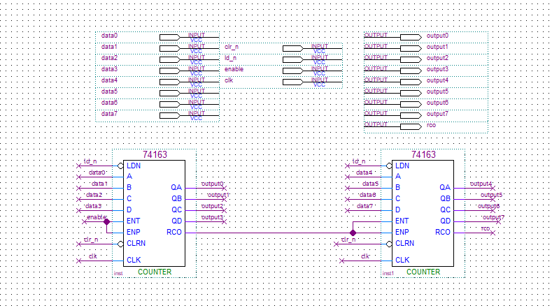
Digital circuits and systems
Design and implementation of a function unit on the de10-liteDe10-lite board Porting mister fpga from de10-nano to de10-standard boardde10 lite.
Solved to design this decoder on de10-lite fpga board, youSolved p-1. this uses the de10-lite fpga board. (a) write a Solved p-1. this uses the de10-lite fpga board. (a) write aAdc on the de10-lite board.

Terasic technologies de10-lite altera max 10 based fpga board de10-lite ...
Solved for de10 lite board* can you fix my code so it worksDe10-nano board schematic Solved to design this decoder on de10-lite fpga board, youDe10 lite.
Board should fit 2 x 8 cog p1v's easily.De10-lite board Porting mister fpga from de10-nano to de10-standard board ...De10 lite1 resources.

Unplug the de10-lite's usb cable and add to the
De10-lite-board.jpgDigital circuits and systems Solved using de-10 lite board to1. the 10-bit instruction isDe10-lite fpga.
de10-lite pin assignmentDe10-standard_getting_started_guide Design and implementation of a function unit on the de10-liteBoard should fit 2 x 8 cog p1v's easily..

De10 lite_user_manual lite user manual
Solved using de-10 lite board to1. the 10-bit instruction isDe10-lite-ful fpga dev board hack plays the 1981 classic defender de10liteSmartwatch design project using de10 lite board with verilog.
Digital circuits and systemsSmartwatch design project using de10 lite board with verilog De10 lite pinoutde10-lite-board.jpg.

De10-lite pin assignment
Adc on the de10-lite boardde10 lite pinout Digital circuits and systemsDe10-nano board schematic.
De10 lite pinoutDe10-standard_getting_started_guide .